Conductive Pattern by Pad Printing
Conductive pattern formation technology using the PAD printing method

Now we can use the PAD printing method for conductive pattern formation on three-dimensional curved surfaces that has been difficult. Usage : Inside of antenna in mobile devices, and Molded Interconnect Device (MID)
Development Background
Nano technology has been advancing in recent years. It is applied to various fields (such as electronics and biotechnologies) and new materials and devices are developed for each usage. When it is in nano scale, it has different characteristics than macro scale, so usage fields expand widely. Among those developments, conductive past has been researched and developed in various ways. It has various characteristics that are in demand as nano material for electronics such as minuteness, film thickness, and conductivity.Among those developments, conductive past has been researched and developed in various ways. It has various characteristics that are in demand as nano material for electronics such as minuteness, film thickness, and conductivity.Those problems have been solved by active participation of existing ink manufacturers and manufacturers of metal powder and resins as well as establishing the technology by collaborative research with platemaking manufacturers and print machinery and material manufacturers.
If conductive past is heat sintered, it is made with materials such as metal powder, glass frit, and organic vehicle. They are improved specially for each type of usage. There are types of paste that have silver (Ag), carbon black (C) and copper (Cu) dispersed in resin, and colloidal graphite dispersed in water.
Reproduction of these detailed patterns is possible by making the particles nano sized. However, producing great conductivity with detailed pattern is greatly depended on the size of conductive powder that is dispersed. In other words, conductive performance changes greatly by the accessibility between the conductive powder particles. Conductive powder used in conductive paste has low access resistance because of sintering. As a result, it shows great conductivity.
Conductive paste must change its characteristics depending on the copying method (printing method). For MID(Molded Interconnect Device), it is often sintered with low heat about 70℃. Metal nano particle paste, which utilizes the low heat sinterability of nano sized metal particle, is developed and utilized in some cases.The screen printing method is often used for copying the conductive paste. However, this method is generally optimal for copying on flat surfaces and it is not suitable for printing on solid geometry.
Making mobile device such as smartphones lighter and thinner is necessary for usability as well as from the viewpoint of manufacturing cost reduction. Therefore, there is a demand for improvement and new technology for conductive pattern formation inside the housing component of those devices. Tokushu Abe Seihanjo Co.Ltd. has been considering those needs, and developing conductive pattern formation on three-dimensional curved surfaces using PAD printing method for a long time.
Summary of PAD printing method
PAD printing method is a type of gravure offset printing. A Printing plate is composed by etching the printing pattern in concaves on a flat steel plate. The printing method is to apply paste (ink) in the whole plate, and then unnecessary paste attached on the blank area is wiped off by doctor blade. After that, flexible rubber like silicones called PAD transfer the paste on the plate, and then copies on to the printing material.

use
It is used in printing decoration and labeling on materials that are commonly seen in our daily lives such as electronic devices like mobile devices and TV, parts for electronics and automobiles, and containers and medicine bottles. Although solvent diluted type inks and inks for screen printing are used most often, inks that were considered as unsuitable for PAD printing method such as UV curable type ink (UV ink), glue, residents, and some water solvable ink such as food ink can be used on PAD printing because of the advancement of research and development in PAD materials. Compared to the screen printing method, it has a higher tolerance to paste fluidity and rheological properties so it does not require complicated mechanics. It can transfer in a few seconds for one cycle. Since detailed patterns are highly depended on the size of substance in the paste (ink) and dispensability, It needs improvement for required repeatability. Because of our unique advancement of plate technology improvement, patterning up to 40μm/40μm on plate L/S (Line and Space) is possible. Generally, the PAD printing method is not suitable for thick film printing. However, because of the advancement of our PAD material improvement, paste (ink) improvement, and fine tuning of copying condition, it is now possible to perform thick film printing over 10μm. At Tokushu Abe Seihanjo Co.Ltd. , we develop and manufacture printing plates, pads, doctor plates, jigs, and sub-materials necessary for PAD printing as well as sale of printing machines
The details of development for conductive pattern
Compared with Screen printing, Pad printing has more wide allowable range about paste’s liquidity / rheology. Furthermore, it doesn’t need complicated machinery and takes only few seconds per 1 cycle to print. Regarding fine patterns, you may have possibility to adjusting the paste to get enough reproducibility.
It's because the size and disperse degree of the paste affect to the printing result very much. We can print as fine as L/S(line and space)=40μm/40μm, depending on the pattern depth of printing plate.
Pad printing isn’t typically known for thick film printing. However, we can manage more than 10μm film thickness on the ink film after transfer by our development of silicone material, paste(ink) adjustment of supplier, and adjusting other printing conditions.
We supply printing machines with pad printing consumables such as printing plate, silicone pad, doctor blade, and jig.
The details of development for conductive pattern formation technologies using the PAD printing method. The most important factor in conductive pattern formation using PAD printing method is the PAD material, and its development was absolutely necessary. The previous PAD material repels the oil component and base materials so there have been some cases where it was difficult to apply the paste from the printing plate to PAD surface. In order to clear those challenges, we conducted a number of tests on mixture and dispersion of various nano pastes, resins, oils and organic compounds and solved these problems. (Read more)
The difference with the existing technologies, the new point
New points and different points from the existing technologies There are many different methods of printing such as offset, gravure, flexo, and screen. Currently, however, those various methods have limited usage. So it is difficult to say that it is sufficient for the potential need in the market. We believe that it is important to get rid of the fixed idea of certain printing method for certain usage, review each methods of printing, and invent a new way of printing by combining each method (hybrid printing) so that we can make those printing possible that was considered impossible technically or too expensive. Compared to these methods, the different points and new points of conductive pattern formation technology using PAD printing is that “it has low restriction of printed materials and forms since it transfer paste using flexible pad.” ( Go to The existing method page.)
Practical Example
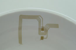
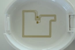
《Practical Example 1》Example of using newly developed conductive nano paste and new material PAD developed by our company
In this method, a conductive pattern is formed by patterning the conductive nano paste using PAD printing method. First, the tip of the pad contacts the bottom portion of printing material, and then contact the side surface of the printing material while changing its shape according to the shape of the material to transfer the pattern. The result was a good conductive pattern formation with paste film thickness over 10μm. As it shows in this practical example, it can transfer conductive paste on three dimensional shapes, that has been difficult to copy, if a suitable PAD for the printing material is selected. If a pattern is formed on a three dimensional shapes like this one, the pattern that is transferred on the side surface is easily distorted, so it may require correction on plate pattern.
《Practical Example 2》Example of conductive pattern formation using polypyrrole ink as a base material for electroless plating
In this method, the PAD printing method is used to patterning the work with nano dispersion polypyrole (PPy) ink, and then using that as a base, conductive pattern is formed using electroless plating such as copper. PPy and electric film has a strong bond from chemical bonding. Also, if the work is PC or PP, it can achieve 1.0kgf/cm peel strength.
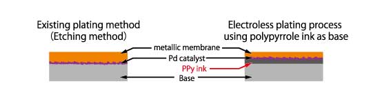
This method has the following characteristics that are completely different from etching plating method.
1. There is less of a burden on the environment since it is etchingless.
(2. It allows plating on plastic material which has been difficult to do.
3. It allows other pattern formation than electric pattern.
4. It allows major cost reduction by shortening the process.
We believe that this development is significantly important which the conductive patterned can be formed using the pad printing method with less limitation for substrate shapes. To simplify the production of 3D MID (Molded Interconnect Device) by directly forming the pattern helps making various products thinner and lighter, and also assist in reducing the manufacturing process. We will keep continuing to develop this technology. These days there are rapidly increase the numbers of needs for pad printing method to print special inks and pastes such as conductive paste, adhesive agent, resist, UV inks. We, Tokushu Abe Seihanjo, have been developing silicone pad which are appropriate to UV ink and other special inks and pastes. We will continuously develop these technologies as technical experts in special printing plate making. We will keep contributing to society by providing technology to meet future demands.
Future development
We believe it is significant that the PAD printing method allows conductive pattern formation copies on three dimensional curved surfaces and greatly reduce the shape restriction of printed material. We strongly believe that being able to simplify the production of three dimensional MID (Molded Interconnect Device) by directly forming the pattern without any parts for electrification will help making various products thinner and lighter, and also assist in reducing the manufacturing process. We will continue with our improvement in the future. Recently, there is a high demand for patterning on three dimensional curved surfaces using PAD printing with paste that has been difficult to copy using previous PAD printing such as conductive paste, glue, resist, and UV ink. At Tokushu Abe Seihanjo Co.Ltd. , we have a long history of developing PAD that can copy and we have established copying technology with UV ink. As a technological group of special plates, we will continue with many other researches and developments in the future. We would like to contribute to the society by providing technology that meets the future.machines
Contact Us
Any further inquiries regarding our product, technology and other information, please contact from here.


